
Getting Your Wafer Temperatures Right (Without the Guesswork)
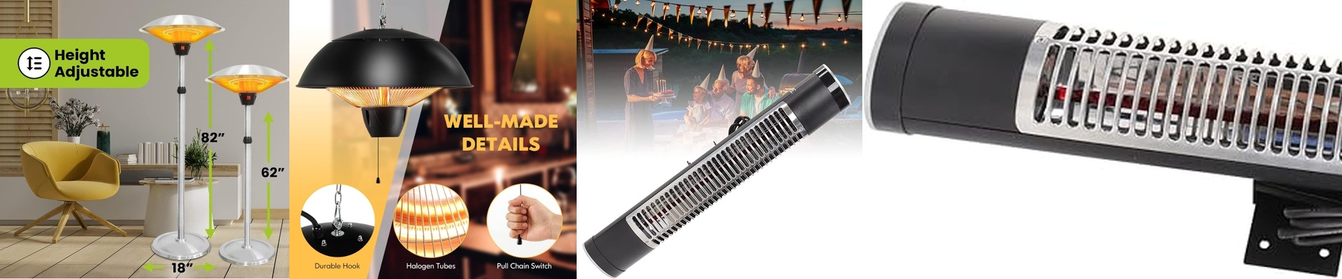
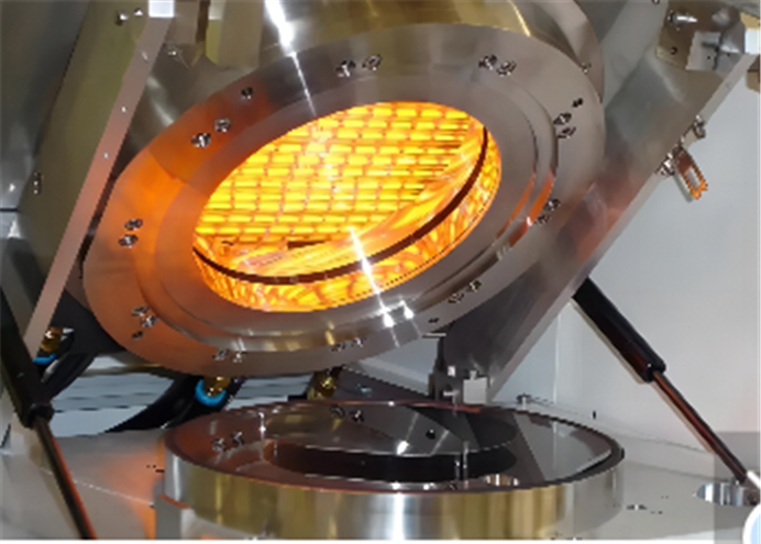
If you’re trying to build a “Smart Fab,” you’ve probably realized that manual sampling is a nightmare. It’s slow, it’s tedious, and frankly, it doesn’t tell you what’s actually happening in the moment. That’s where high-precision IR sensors come in. They let us see the thermal profile of a 300mm wafer in milliseconds, all without ever touching the substrate. It’s the only way to get that kind of speed and accuracy. How it actually works Here is the deal: these sensors pick up the electromagnetic radiation coming off the wafer’s surface. Instead of a technician scribbling notes, the raw data flows straight into your PLC or SCADA system. You can see the temperature uniformity across the whole wafer as it happens. If a hot spot pops up, the system catches it and tweaks the heating elements instantly. No more crossing your fingers and hoping the batch comes out right. Making the hardware play nice For a Fab to actually feel “smart,” your gear needs to talk to each other. We make sure our IR systems use standard signals—usually 4-20mA or digital protocols—so they just plug right into your existing data backbone. This creates a closed-loop. You aren’t just staring at a screen watching the heat rise and fall; you’re using that live data to actually drive the machine. The reality check Now, I’ll be honest: high-res IR sensing isn’t a magic wand you just wave over every tool. These sensors need a clear line of sight. If your chamber has vapor or gunk building up on the viewport, your readings will start to drift. It’s frustrating, but it’s physics. You have to plan for it. Whether that means a strict maintenance schedule for the optical path or installing a purging system to keep the lens spotless, you’ve got to do it. Because if the window is dirty, your “smart” data is basically just noise. It’s a bit of extra work, but that’s the price you pay for the kind of precision semiconductor work demands.