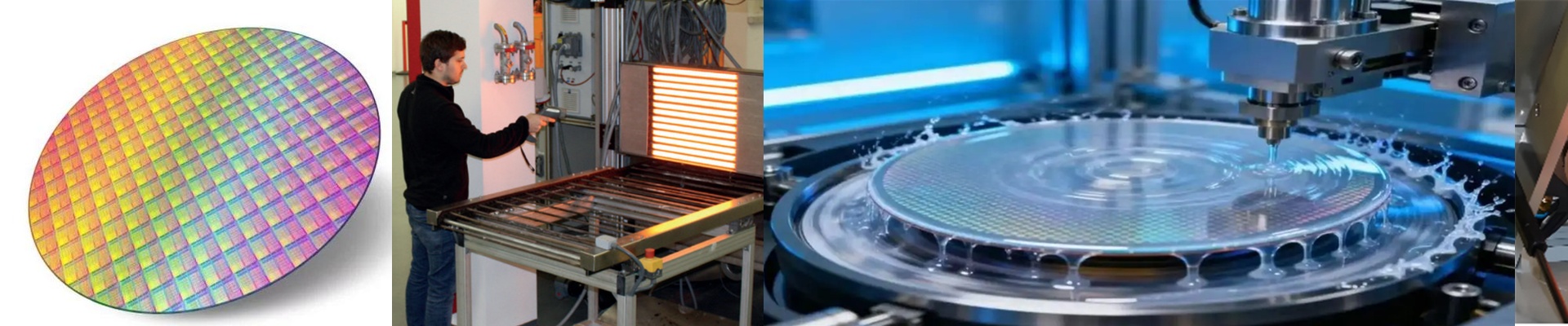
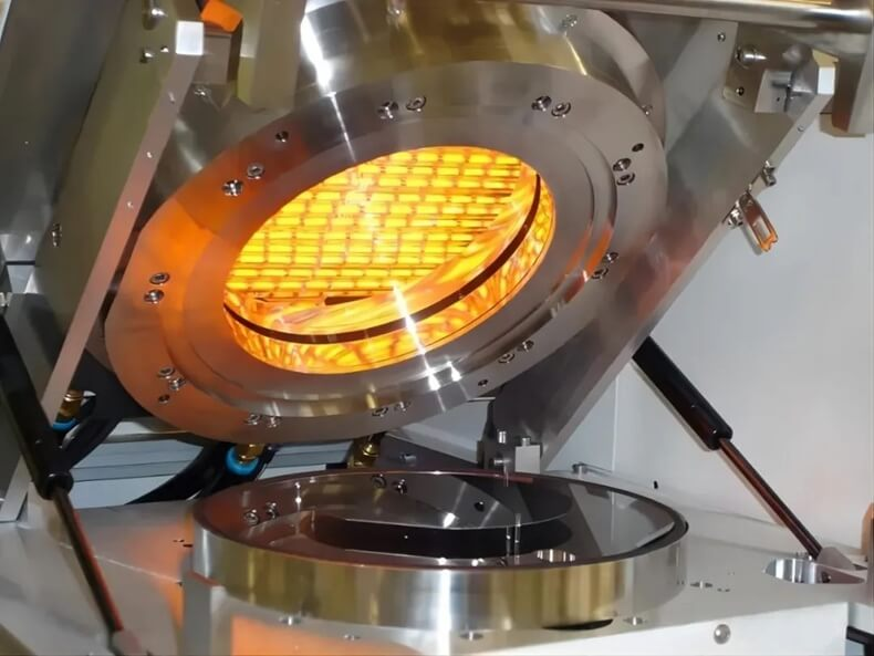
On the fab floor, a cleaned wafer is only as clean as its final drying step. Water marks, micro-particles, and photoresist adhesion issues all trace back to thermal profiles that are inconsistent or contaminating. After the wash, there’s no room for guesswork. What matters technically We build the drying step around controlled heat delivery. Our NIR-based systems hold ±0.1°C wafer-level thermal uniformity, so evaporation stays consistent across the entire surface. Cleanroom compatibility is baked in — Class 1–100 environments, zero particle generation, and sealed thermal paths. The outcome is repeatable sub-monolayer residue removal without stressing the stack. Why it works in practice After cleaning, the wafer has to hit lithography or photoresist processing with a pristine, dry surface. This approach keeps the critical process windows intact: soft bake and hard bake temperatures stay within spec, line-width control holds steady, and defect rates drop. The system runs 24/7 with zero unplanned downtime, and energy use stays predictable — keeping thermal budgets tight and cycle times short. What to keep in mind NIR drying is fast and clean, but it needs precise line-of-sight alignment and stable substrate geometry. Existing tracks require a calibrated interface to match wafer positioning and exhaust capture. Plan for a short integration window and a validation run focused on particle count and temperature profile. Get those two items right, and the drying step stops being a risk. It becomes a controllable process knob you can trust.